Electronics Production

Week 4

Assignments

Group Assignment
  • Characterize the design rules for your PCB production process
Individual Assignments
  • Make an in-circuit programmer by milling and stuffing the PCB, test it, then optionally try other PCB processes
  • I was in the group with Antti Rytilahti and Kenichi Komatsu and after our local instructor's lecture (Antti), we started to work with different mode operation and milling bits to characterize and try different setting to see the changes of the results. Please find more detils of our group assignment here.

    Making .rml files in mods:

    First of all, we will need png or svg file formats to .rml files for PCB millings for traces and outlines.

    Go to mods to generate .rml files

    • Right click > program> open server program > Roland> SRM-20 > PCB svg
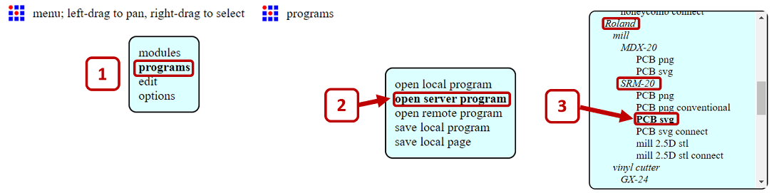
    • Figure 1. Opening svg file in mods

    • Delete WebSocket Serialwhich is not goinmg to be used.
    • Then, right click > modules > open server module > file (save) and connect it to the output of Rolland SRM-20 milling machine. This will create the save node and the files will be automatically dowlnaded on you PC .
    • In Rolland MDX-20 milling machine module, Set the origin coordinates to (x=0, y=0, z=0).

    Traces

    • Go to read SVG > Select SVG file and upload the file. Press view and invert the image to see the coppertraces white, while isolation is black.
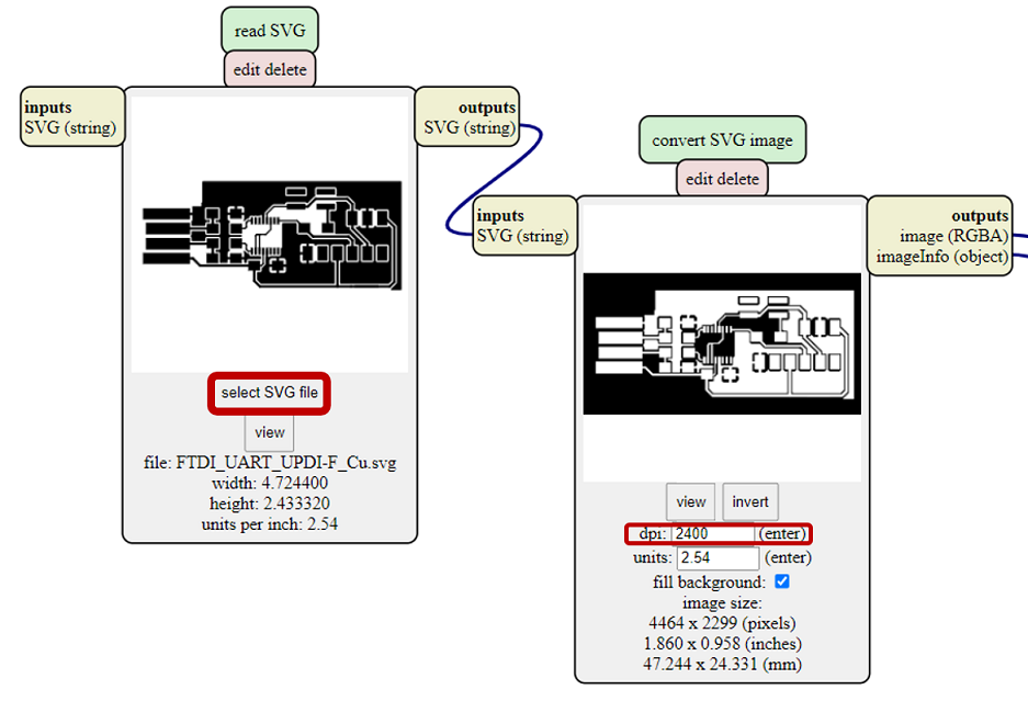
    • Figure 2. Inverting png file in mods

    • Go to Set PCB defaults> mill traces 1/64 for outlines .
    • Go to Mill raster 2D> tool diameter and try to find the optimum amount (0.2 - 0.5 mm V type) with checking view toolpath.
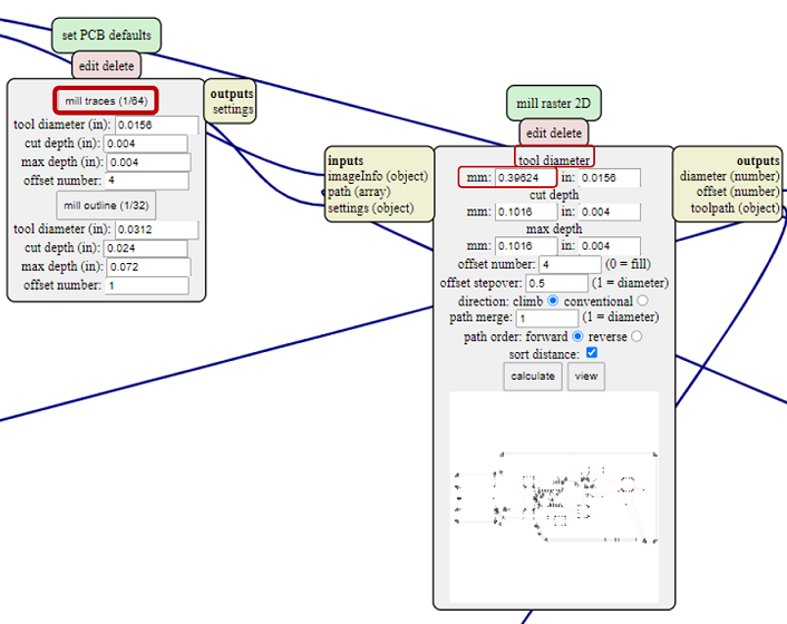
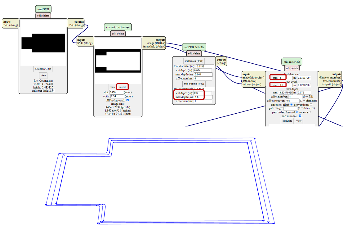
    • Figure 3. Setting preparation for tracing in mods

      For the default amount of tool diameter (0.39624 mm), there are some missing lines in toolpath view (Figure 4). So, I tried 0.25 mm and finally, 0.22 mm which had the finest drawing. It is better to start with the higher number since more copper will be removed.

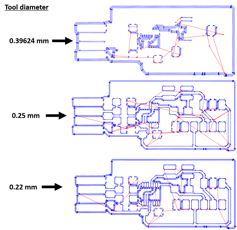
      Figure 4. Comparision of different tool diameter in toolpath view

    • Set Offset number as 4
    • Finally, press Calculate which will generate .rml file and automatically save it.
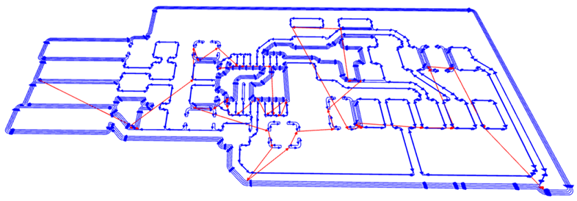
    • Figure 5. Generated .rml file of tracing for PCB milling in view mode

    Milling PCB

    First, the milling machine (Roland SRM-20) should be callibrated and for that, we performed these following steps on PCB board and the milling machine:

    • The blank PCB to cut was selected form FR-1. First of all, we should be sure of the flatness of the surface. We can test it with a ruler putting on the side of the blank and check if there is a gap between them or not. Since we used a big piece of blanck to get four board cut from it, it was a bit tricky to have all the surface flattened
    • There should not be any dust on the surface, so you can use a wet cloth to clean it. Then, we applied Isopropanol to clean adhesive residue from the previous double sided tape. The material should be fixed to the stage inside the machine. So, we used doudble-side tape to cover the whole back surafce of the blank but you should be very careful not to have bubbles.
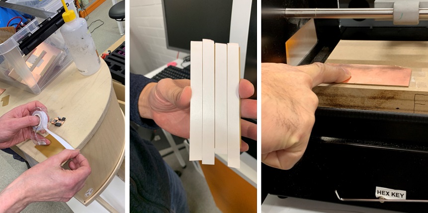
    • Figure 7. Double sided tape on the back side of the blank PCB

    • For the milling bit, I used V shape 0.2-0.5 mm milling bit for Traces and Calibraion while for Outline, flat 1 mm bit was used. To install the chosen bit into the machine, you should hold it with your finger and be very careful not to drop it since they are very sensitive and might be broken. Then, place it to the collet and tight it with a hex key carefully since extra pressure may cause the break.
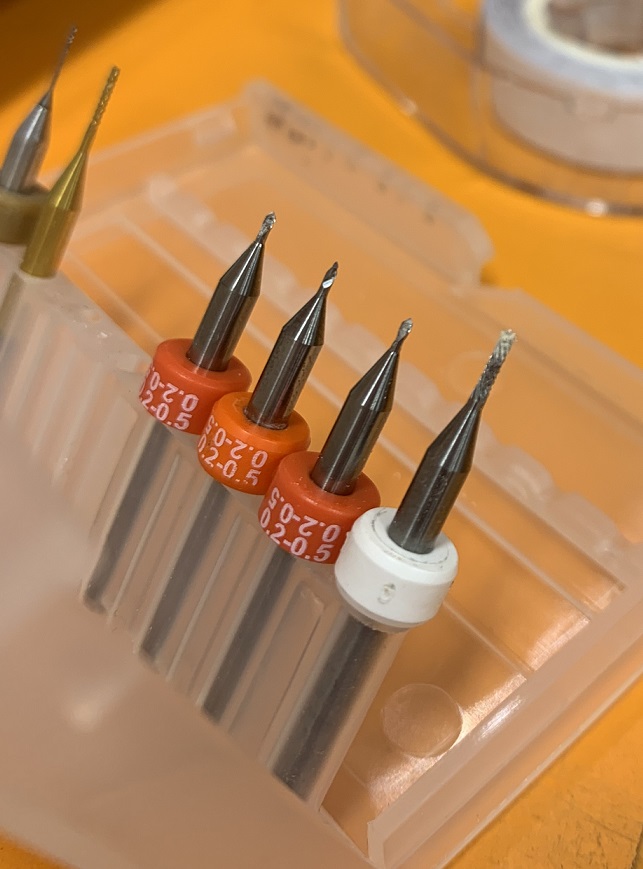
    • Figure 8. Different milling bits with different shape and thickness

    Vpanel for SRM-20

    To start and set the softwate Vpanel for SRM-20, we followed the following steps:

    • Set the Origin for X, Y and Z. Cursor steps are optional: continious mode or jogs by 1 mm, 0.1 mm or 0.01 mm (*100, *10 and *1, respectively). The default origin of the blank is left botton corner. First, set the origin for XY position (from Set Origin Point> User coordinate system).
    • Then, move slowly along the Z axix untill about 1 mm to the surface of the blank, untight the collet and carefully, let the milling bit touch the surface and tight it again. Now, you can set the origin point to Z.
    • Finally, when you are sure of the origins have been correctly set, you can press Cut button and add the .rml file you are going to cut. But before that, delete any previous file. Then, press Output and now, cutting will be started. You can press PAUSE to check the milling quality with by pressing View button.
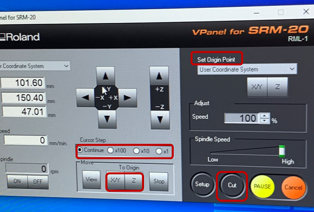
    • Figure 9. Settings in Vpanel for SRM-20

    • Since we were going to cut four board from the selected blank PCB, we had to keep a track of the previos XY set origins and adjust the next board according to those measures. The firt board was cut perfectly, but for the rest, we had some problems to find the proper Z origin since the machine was milling in the air or not very deep on the surface. But after several tests, we succeeded to cut two more PCB.
    • For cutting Outline, we used 1 mm bit
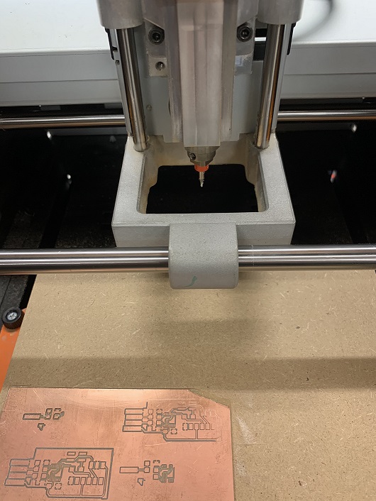
    • Figure 10. Milling several boards on the blank with different Z origin

    • After cutting process was finished, the milling boards were smoothly removed from the stage by a spatula.
    • Figure 11. Removed cutting boards from the blank

    • Now, it is the time to clean the board gently by scrubbing PCB surface with a steel wool. to protect copper from oxidation, front contacts using for USB port were covered with a thin layer of tin.

    Soldering and assembling components

    Soldering was the most difficult and time-consuming part of this week task for me since I had absolutely zero experience in it and also, I was super cautious and afraid not to overheat anything!

    An image of the whole setup we used is presented in Figure 12 and it was included of the following items:
    • Soldering iron set at the temperature 350 Celcius
    • Solder wire (tin metal)
    • Fume extractor which is a system that utilizes a fan using a negative draft to pull fumes and dust particles in to a contained filtration system.
    • Microscope to examine the details of seldering quality
    • Desoldering Braid to absorb excess soldering
    • The components to be assembled and soldered on PCB
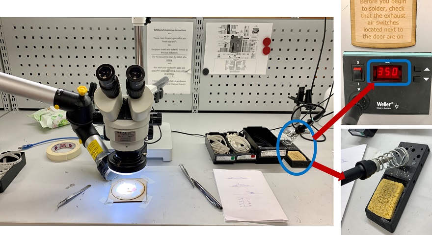
    • Figure 12. Soldering setup

    We had a picture of the final board as a refernce to know the position of each component.

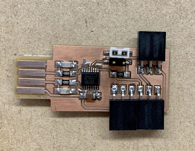
    Figure 13. The reference PCB

    Finally, after several hours and with the help of our local instructor (Antti) and my groupmate (Antti :D), I succeeded to finish soldering and PCB was ready to test.

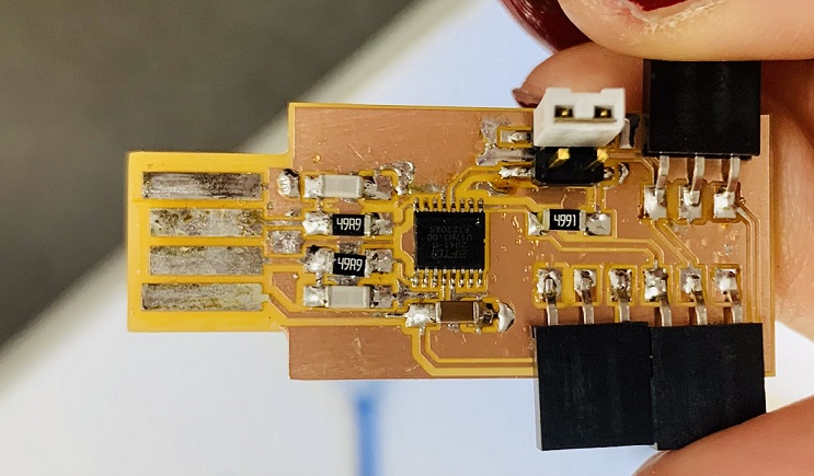
    Figure 14. My soldered PCB is ready!

    Testing the board

    After installation of Arduino, open it and for further instruction, go to this page and install megaTinyCore board manager as the folloewing:

    • Go to File > Preferences, enter http://drazzy.com/package_drazzy.com_index.json in Additional Boards Manager URLs
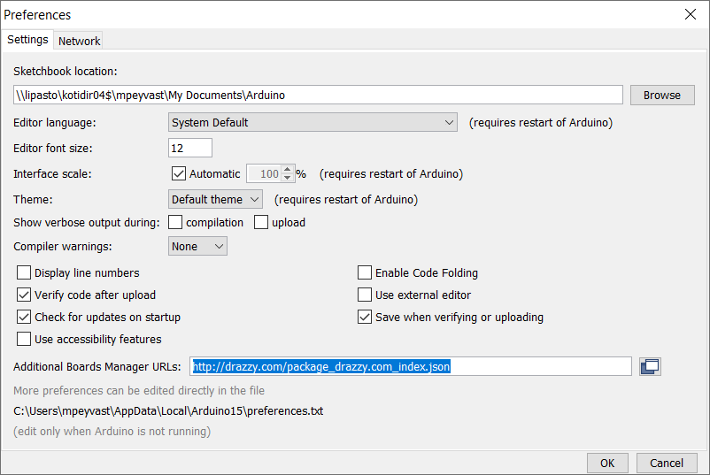
    • Figure 15. Installing megaTinyCore board manager in Arduino

    • Go to Tools -> Boards -> Boards Manager, then, select "megaTinyCore by Spence Konde" and click Install.

    Then, in Arduino IDE, copy-paste the hello.t412.echo.ino sketch here .

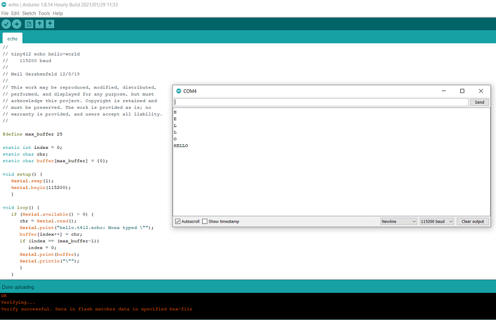
    Figure 16. Uploading and testing the sketch in Arduino IDE

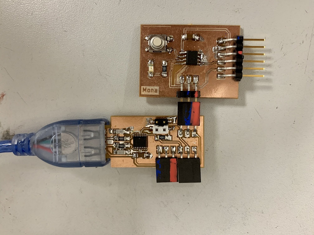
    Figure 17. Attaching the board to the programmer and USB connection

    After installing PuTTY, open it and set the serial with a new name (COM4 for my case).

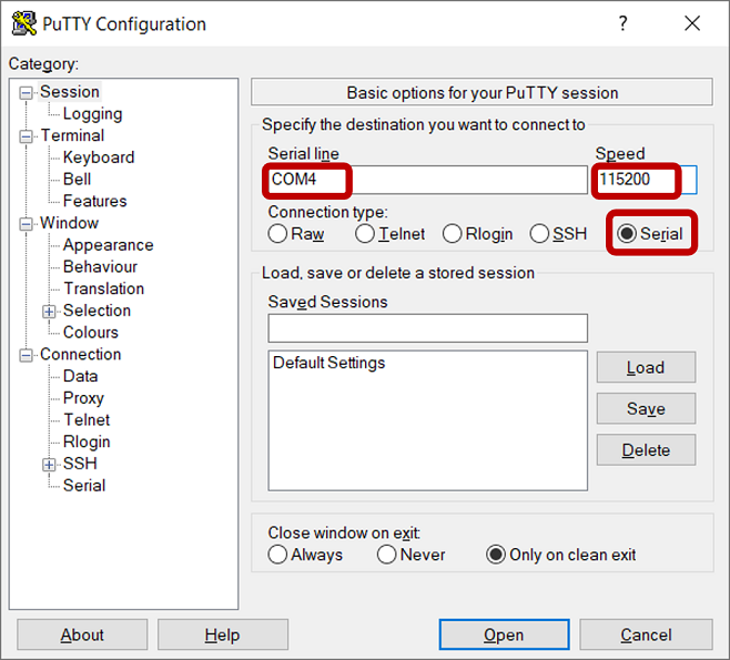
    Figure 18. PuTTY settings

    Now, connect the board to the programmer and attach it to the usb cable. Then, click Open and just type something to see if it has been programmed correctly.

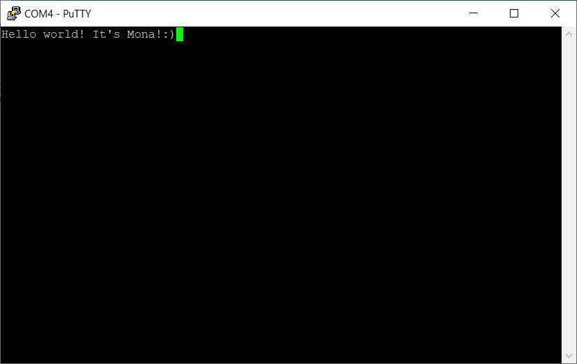
    Figure 19. Testing the programmed board

    Then, disconnect the programming board and connect the ATtiny412 microchip board via USB cord.

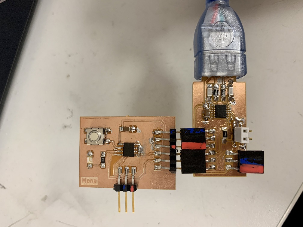
    Figure 20. Connecting the ATtiny412 microchip board via USB cord

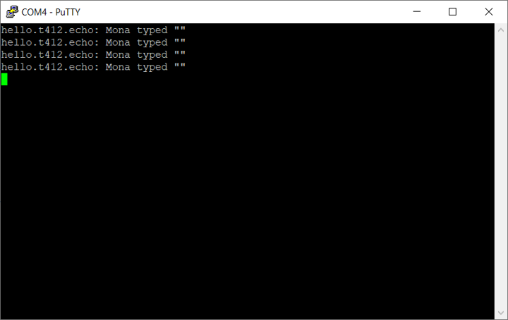
    Figure 21. Testing the echo sketch on the programmed board.

    For documentation of this week, I have taken hints from many webpages of the former students of Fablab, especially (Arash , Gleb and Tatiana) in addition to my memory and notes from the lectures!

    Reflection

    Since I had zero experience in making boards and in general, in electronics production, I was terrified of this week in advance:D But with thourough instructions and patience of our local instrictor, Antti, I did not face serious problem excep for soldering. Since I had never done soldering before, I was super cautious and afraid of overheating the components. So, I did not solder enough and therefore, I had to do it several times to have a fine soldering without any short circuit.

    Files

    Mona Peyvasteh

    Fab Academy 2021

    Diary of my journey to the world of Digital Fabrication